structural and electronic properties of silicene in the presence and absence of vacancy
Adnan Rhaif Lahoo Alzayadi
Education Directorate of Al Muthanna
009647802678867
adnanalzayadi99@gmail.com)
Ebrahim Safari
Tabriz University – Faculty of Physics
Abdollahi pour
Tabriz University / Faculty of Physics
Abstract:
In this research, the electronic and structural features of silicene nano sheets in the presence of vacancies were investigated according to density functional theory. The calculations were performed using Siesta code and GGA-PBE approximation. Examination of the relaxed structure of silicene monolayers shows that it has a quasi-planar structure. Due to the band structure and total density of states of silicene it can be considered as semi-metal because its energy gap is zero. Examination of the band structure and total density of states of the 2×2 super cells in the presence of a vacancy indicates that the presence of a vacancy has opened the band gap in the silicene structure and its band gap is indirect.
Key words: Silicene, density functional theory, structural properties, honeycomb structure
الخواص البنيوية والإلكترونية للسيليسين في وجود الشواغر وغيابها
عدنان رهيف الزيادي
مديرية التعليم المثنى – العراق
009647802678867
adnanalzayadi99@gmail.com
إبراهيم سفاري
جامعة تبريز – كلية الفيزياء – ايران
عبد الله بور
جامعة تبريز / كلية الفيزياء- ايران
ملخص:
تم في هذا البحث دراسة الخصائص الإلكترونية والتركيبية لصفائح السيليسين النانوية في وجود شواغر وفق نظرية الكثافة الوظيفية. تم إجراء الحسابات باستخدام كود Siesta وتقريب GGA-PBE. يُظهر فحص البنية المريحة لطبقات السيليسين الأحادية أن لها بنية شبه مستوية. نظرًا لبنية الشريط والكثافة الإجمالية لحالات السيليسين، يمكن اعتباره شبه معدني لأن فجوة الطاقة فيه تساوي صفرًا. يشير فحص بنية النطاق والكثافة الإجمالية لحالات الخلايا الفائقة 2 × 2 في وجود وظيفة شاغرة إلى أن وجود وظيفة شاغرة قد فتح فجوة النطاق في بنية السيليسين وأن فجوة نطاقها غير مباشرة.
الكلمات المفتاحية: السيليسين، نظرية الكثافة الوظيفية، الخواص التركيبية.
Introduction:
A Silicene plate is made by extracting an atomic single layer from silicon and deposited on the Ag (111) surface [1- 4]. The first reports and theoretical studies were made by Vikkeda -shirashi [5], in which the electronic and crystalline structure of isolated Silicene was investigated. The first synthesis on Ag (111) was done in 2010 by Chemical vapor deposition (CVD) method [6]. Silicene has a 2D honeycomb structure with a small bending [7]. The buckled structure of Silicene is a unique feature that make it possible to change the band gap of the material without changing the chemical potential and only by applying an external electric field. The band structures represent the energy levels that the electron can have with the K wave vector. The electronic band structure of two-dimensional honeycomb Silicene is drawn in the high symmetry directions K (1.0,0.5,0), M (0.6,1.1,0), Γ (0,0,0) in the first Brillion zone [8, 9]. According to the band structure energy gap is zero, and conduction and valance bands cross each other at the Dirac point K (the Dirac point is a location in the Brillouin zone where the conduction and valence bands cross each other). Moreover, it implies that the density of states in the Fermi energy is zero, therefore Silicene can be considered a quasi-metal [10, 11].
Calculation methods
All calculations have been done using the density functional theory and under Siesta code [12-15]. In input file there is information about the structure of the molecule, the number of atoms in the first Brillouin zone, the type of molecules and the coordinates of atoms. The file related to quasi-potential is predicted according to the type of atoms in the program. According to Figure (1), the optimal cut-off energy for integration in real space for single-layer silicene structure was chosen equal to 250 Ry. To describe the Brillouin zone, the optimum k points according to Figure (2) were considered equal to 20×20×1 based on the Monkhorst-Peck method. The optimized lattice constants for silicene single layer are drawn in figures (3) and (4).

Figure (1). Optimization of cut off energy for silicene monolayer
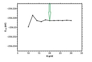
Figure (2). Total energy changes with the number of k points in silicene monolayer

Figure (3). Optimization of lattice constants of silicene single layer in the x-axis direction
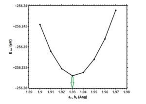
Figure (4). Optimization of lattice constants of silicene single layer in the y-axis direction
As it is clear in these figures, the optimum lattice constants of silicene monolayer are:
ax = 3.45Å, ay = 1.93Å
bx = 3.45Å, by = 1.93Å
The lattice constants and assortment of all atoms were weakening until the force on each atom was less than 0.01 eV/Å. To prevent possible interactions with the neighboring layers, a sufficiently large vacuum layer was included in the non-periodic orientations.
Results and discussion
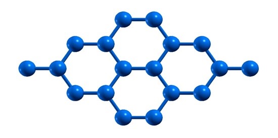
The geometric texture of the silicene unit cell (a) and the silicene monolayer after relaxation are shown in figure (5). Examination of the obtained texture shows that silicene has a quasi-planar structure and the bending value of the structure is equal to 0.39Ao. The bond length between silicon atoms is equal to 2.33Ao.
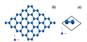
Figure (5). (a) Geometrical structure of silicene unit cell, (b) silicene monolayer from the top view
Electronic calculations include energy band structure and density of states. From the band structure, we can obtain the conductivity properties of materials, size and location of gaps, the Fermi energy and the degeneracy of the system. To better understand the electronic features of silicene, it is useful to draw the electronic band structure, after obtaining the Hamiltonian matrix by self-consistent solution method. Now with eigenvalues, we can draw the band structures. Electronic band structure of two-dimensional honeycomb silicene in high symmetry directions K (0.68, 0.32, 0.0), M (0.5, 0.5, 0.0), Γ (0.0, 0.0, 0.0) is drawn in the first Brillouin zone; The location of these symmetric points in the first hexagonal Brillouin zone of silicene is shown in Figure (6). The density of states of silicene monolayer is drawn in figure (7). Fermi energy is chosen at the zero point. According to the band structure obtained in figure (6), silicene can be considered as a quasi-metal because the energy gap is zero and the conduction band and valence band intersect at the Dirac point K. In addition, according to figure (7), the value of the density of states in the Fermi energy EF is zero.
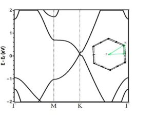
Figure (6). band structure of silicene monolayer. The Fermi energy is chosen at the zero point.
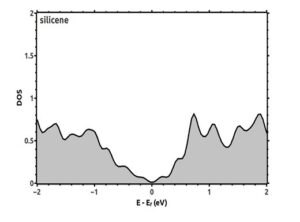
Figure (7). Total density of states of silicene monolayer. The Fermi energy is chosen at the zero point.
Moreover, 2×2 and 3×3 supercells of silicene were selected and its structure was relaxed with the same parameters as the silicene monolayer. The geometric structure of the 2×2 and the 3×3 supercells of silicene after it has been relaxed are shown in figures (8) and (9), respectively.
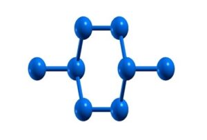
Figure (8). The geometric structure of the 2×2 supercell of silicene after relaxation

Figure (9). The geometric structure of the 3×3 supercell of silicene after relaxation
A vacancy was created in each of the 2×2 and 3×3 supercells and the structures were relaxed with the previous parameters. The curvature value of the structure in the presence of vacancies has increased significantly. In the 2×2 supercell, the curvature value is 1.27 Å and in the 3×3 supercell, it is 1.57 Å.
The band structure of a 2×2 supercell of silicene in the presence of a vacancy is shown in Figure (10). According to the figure, it can be seen that the presence of vacancies has caused the opening of the band gap of 0.48 eV in the silicene structure and its band gap is indirect.
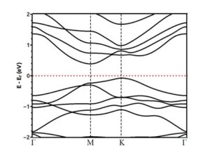
Figure (10). Band structure of a 2×2 supercell of silicene in the presence of a vacancy
Figure (11) show the band structure of a 3×3 supercell of silicene in the presence of a vacancy. According to the band structure, it can be seen that the presence of a vacancy in the 3×3 supercell has also caused the opening of an indirect band gap of 0.03 eV in the silicene structure.
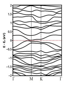
Figure (11). Band structure of 3×3 silicene supercell in the presence of a vacancy.
The total energy value of the studied structures is reported in Table (1). All obtained values are negative, which indicates the stability of the studied structures. Among the investigated structures, the 3×3 supercell of silicene is more stable than the others in the presence of a vacancy.
Table (1). Comparison of the total energy of the studied structures.
| structure | Total energy (eV) |
| Silicene monolayer | -213.85 |
| The 2×2 supercell of silicene in the presence of a vacancy | -769.51 |
| The 3×3 supercell of silicene in the presence of a vacancy | -1868.69 |
Conclusion
In this research, the textural and electronic features of silicene monolayers in the presence of vacancies have been investigated using the Siesta computational code in the framework of the density functional theory and using the generalized gradient approximation.
The obtained results show that the silicene monolayer has a quasi-planar texture and the structure curvature is 0.39 Å. Examining the band structure and total density of states of silicene monolayer shows that this structure has quasi-metallic behavior. It exhibits semiconducting behavior in the presence of a vacancy. Negative values for the total energy of silicene monolayers shows that all the investigated structures are stable.
References:
[1] Martin, R.M. (٢٠٠٤). Electronic Structure – Basic Theory and Practical Methods Cambridge University Press.
[2] W. Kohn, “Nobel lecture: Electronic structure of matter—wave functions and density functionals,” Reviews of Modern Physics, vol.71, no.5, p.1253, 1999.
[3] Yukiko Yamada-Takamura and Rainer Friedlein, “Progress in the materials science of silicene” National Institute for Materials Science Science and Technology of Advanced Materials Sci. Technol. Adv. Mater. 15 (2014) 064404 (12pp).
[4] B. Mohan, A. Kumar, P. K. Ahluwalia, “Low-dimensional Systems and Nanostructures”, Physica E 44 (2012) 1670
[5] K. Takeda and K. Shiraishi, “Theoretical possibility of stage corrugation in Si and Ge analogs of graphite”, Phys. Rev B 50 (1994) 14916.
[6] G. Liu, M. S. Wu, C. Y. Ouyang and B. Xu. “Strain-induced semimetal-metal transition in silicene”, epl gournal. 99 (2012)17010
[7] Jose, Deepthi, and Ayan “Data.Accounts of chemical Research” 47 (2013) 2.
[8] S. Cahangirov et al.,” Two- and One-Dimensional Honeycomb Structures of Silicon and Germanium”, Phys Rev Lett 102 (2009) 236804.
[9] H. S¸ahin, S. Cahangirov, M. Topsakal,E. Bekaroglu, E. Akturk, R. T. Senger,2 and S. Ciraci. “Monolayer honeycomb structures of group IV elements and III-V binary compounds”, arXiv:0907.4350v1 [cond-mat.mtrl-sci] 24 Jul 2009.
[10] Rui Qin, Wenjun Zhu, Yalin Zhang and Xiaoliang Deng. “Uniaxial strain-induced mechanical and electronic property modulation of silicone”, Nanoscale Research Letters 2014, 9:521
[11] Huijuan Zhao. “Strain and chirality effects on the mechanical and electronic properties of silicene and silicane under uniaxial tension”, Physics Letters A 376 (2012) 3546–3550
[12] Soler, J.M., Artacho, E., Gale, J.D., García, A., Junquera, J., Ordejón, P., Sánchez-Portal, D., “The SIESTA method for ab initio order-N materials simulation”, J. Phys. Cond. Matt., Vol. 14, 2002.
[13] Perdew, J.P., Burke, K., Ernzerhof, M., “Generalized Gradient Approximation Made Simple”, Phys. Rev. Lett., Vol. 77, 1996.
[14] Yukiko Yamada-Takamura and Rainer Friedlein, “Progress in the materials science of silicene” National Institute for Materials Science Science and Technology of Advanced Materials Sci. Technol. Adv. Mater. 15 (2014) 064404 (12pp)
[15] G. Liu, M. S. Wu, C. Y. Ouyang and B. Xu, “Strain-induced semimetal-metal transition in silicene”,epl gournal . 99 (2012)17010